

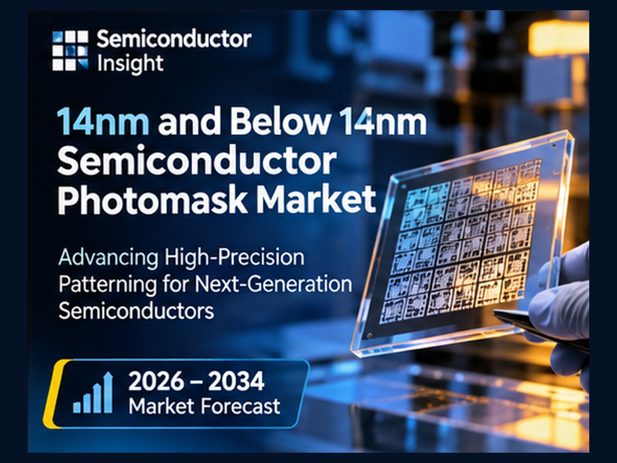
14nm and Below 14nm Semiconductor Photomask Market to Reach USD 5.89 Billion by 2034 as Advanced-Node Chip Production Expands

The semiconductor industry is moving toward increasingly advanced process technologies as demand grows for high-performance computing, artificial intelligence and next-generation connectivity. Within this environment, semiconductor photomasks remain essential to transferring complex circuit patterns onto silicon wafers, particularly for logic and memory devices manufactured at advanced nodes.
According to Semiconductor Insight, the Global 14nm and Below 14nm Semiconductor Photomask Market was valued at USD 3.42 billion in 2025 and is projected to grow from USD 3.68 billion in 2026 to USD 5.89 billion by 2034, exhibiting a CAGR of approximately 6.1% over the 2026–2034 forecast period. The market includes qualified photomasks used for 14nm, 7nm and below-7nm semiconductor processes, including binary, phase-shift and EUV reticles.
Explore the complete 14nm and Below 14nm Semiconductor Photomask Market analysis: https://semiconductorinsight.com/report/14nm-and-below-14nm-semiconductor-photomask-market/
Why Are Advanced-Node Photomasks Important in Semiconductor Manufacturing?
Photomasks are optical masters carrying circuit patterns used to expose photoresist on silicon wafers. At 14nm and below, the masks require refined optical proximity correction, electron-beam writing, defect detection and dimensional control to reproduce increasingly complex layouts.
The advanced-node segment includes masks for 14nm, 7nm and sub-7nm processes. These generations support higher transistor density and improved performance in modern processors, networking chips, AI accelerators and advanced smartphones.
EUV reticles use reflective multilayer structures, while 193nm deep-ultraviolet processes may use transmission masks and multiple aligned exposures. The technology selected depends on the target process, design rules and lithography flow.
Because a defect on a reticle can be repeated across many dies, manufacturers place strong emphasis on pattern registration, inspection, repair and traceability. These requirements make qualified photomasks a critical part of advanced semiconductor production.
Market Growth Is Closely Linked to Advanced Semiconductor Demand
One of the major trends influencing the 14nm and Below 14nm Semiconductor Photomask Market is increasing demand for high-performance computing, artificial intelligence and 5G technologies. These applications require advanced chips with dense circuit patterns and demanding performance characteristics.
Semiconductor Insight identifies growing demand for advanced semiconductor fabrication as a key market driver. As foundries and integrated device manufacturers develop smaller process technologies, the need for qualified reticles and repeated mask revisions increases.
The market is also supported by investments in semiconductor manufacturing capacity. Taiwan, South Korea, Japan and China form important parts of the regional ecosystem, while North American chip design and manufacturing programmes contribute to demand for advanced masks.
The shift toward 7nm and below technologies can increase mask complexity through additional pattern correction, inspection and EUV integration. These factors support the value of advanced photomask solutions across the forecast period.
EUV and Advanced Mask Technologies Are Reshaping the Market
The market is segmented by process generation into 14nm nodes, 7nm nodes and below-7nm nodes. Each category has different requirements for pattern fidelity, exposure methods, inspection and qualification.
At 14nm, photomasks commonly support 193nm immersion exposures and optical proximity correction across multiple layers. Established production experience helps maintain process consistency, while new processor and networking designs continue to generate mask orders and revisions.
The 7nm generation requires denser features and more aggressive image correction. Some manufacturing flows combine multiple DUV patterning steps with EUV on selected critical layers, making reticle qualification and defect control increasingly important.
Below-7nm designs, including nominal 5nm, 3nm and emerging 2nm processes, increasingly use EUV reflective masks and complex corrections. High-quality blanks, absorber control, pellicle compatibility and inspection capability remain important technology requirements.
View the complete 14nm and Below 14nm Semiconductor Photomask Market segmentation and forecast: https://semiconductorinsight.com/report/14nm-and-below-14nm-semiconductor-photomask-market/
Logic Devices and Foundry Services Create Major Demand
Logic devices represent the largest application category in the report, supported by processor, GPU, AI-chip and networking-ASIC designs. Each design iteration may trigger reticle changes even before high-volume wafer shipments begin.
Foundry services represent another important application because external wafer manufacturers support multiple fabless customers. The commercial cycle includes tape-out, mask-data preparation, reticle qualification and revisions required for yield or functionality.
Memory devices also require accurate reticles for advanced DRAM and selected high-density memory production. Their procurement economics differ from custom logic because memory manufacturers often optimise a smaller number of highly repeated layouts.
Integrated device manufacturers contribute through internal mask operations and specialist outsourcing. Their mask requirements are linked to qualifying semiconductor processes rather than the full cost of operating a fabrication facility.
Asia-Pacific Manufacturing Clusters Support Market Expansion
Asia-Pacific is the largest regional market, accounting for an estimated 61% of 2025 value. Taiwan, South Korea, Japan and China concentrate advanced wafer fabrication, photomask writing and related materials capabilities.
Taiwanese foundries and chip-design customers generate demand for reticle sets at 7nm and below. Japan contributes specialist mask production and EUV blank technologies, while South Korea supports demanding memory and logic manufacturing environments.
North America represents an estimated 22% of the market, supported by processor design, high-performance computing and selected domestic semiconductor production. Europe accounts for approximately 12%, with strengths in mask-writing expertise, inspection technologies and collaborative research.
The Middle East and Africa and South and Central America represent smaller emerging markets. Their participation is more closely associated with design, research and overseas foundry access than with large-scale local production of leading-edge reticles.
High Production Complexity and Defect Control Remain Challenges
Advanced photomask production requires specialized writing, inspection and repair equipment. Multibeam electron-beam writing, blank quality and inspection throughput can influence production capacity and turnaround times.
EUV masks introduce additional requirements involving reflective multilayer structures, absorber control and pellicle compatibility. Defects must be detected and managed carefully because a single reticle issue can affect many high-value semiconductor dies.
Mask makers also handle confidential design files through tightly controlled data preparation, writing, etching, inspection and repair workflows. Protecting intellectual property and maintaining traceability are important parts of supplier qualification.
Access to advanced tools and qualified production capacity can constrain suppliers. The transition toward future mask formats remains a development programme and should not be confused with established volume production.
Where Are the Biggest Opportunities Emerging?
The migration toward 7nm and below process technologies creates opportunities for suppliers capable of supporting complex EUV and DUV mask requirements. Higher-resolution correction and demanding inspection specifications can increase the value of qualified reticles.
AI accelerators, advanced processors and networking ASICs are important downstream applications because their designs require precise patterns and repeated engineering updates. These product cycles support demand for specialist mask-writing services.
Investment in multibeam writing, inspection and EUV blank capacity can strengthen supplier capability. Regional projects in Asia, Europe and North America may improve access to advanced mask services and support supply-chain resilience.
Future high-NA EUV development and proposed larger mask formats represent longer-term opportunities. Their commercial contribution will depend on successful qualification, equipment readiness and adoption by leading-edge wafer manufacturers.
Receive your Free Sample Report today: https://semiconductorinsight.com/download-sample-report/?product_id=135744
Cost, Qualification and Industry Development Considerations
Market participants must evaluate technology performance alongside manufacturing economics, qualification requirements and customer demand. Suppliers that can demonstrate reliable production, consistent quality and compatibility with established workflows are better positioned to support adoption.
The report’s market outlook reflects the interaction of technology development, investment decisions and end-user requirements. Adoption may vary across product categories and regions depending on manufacturing readiness, supply availability and the economics of deployment.
14nm and Below 14nm Semiconductor Photomask Market Segmentation
The report evaluates the market by product type and application, providing a detailed view of where demand is developing.
By type, the market is divided into:
14nm Nodes
7nm Nodes
Below 7nm Nodes
By application, the market covers:
Logic Devices
Memory Devices
Foundry Services
IDM Production
This segmentation reflects the different patterning and qualification requirements across semiconductor process generations and customer types. Mask value is influenced by design complexity, correction workload, inspection specifications, turnaround time and the level of process integration required.
View the complete 14nm and Below 14nm Semiconductor Photomask Market segmentation and forecast: https://semiconductorinsight.com/report/14nm-and-below-14nm-semiconductor-photomask-market/
Regional 14nm and Below 14nm Semiconductor Photomask Market Outlook
Asia-Pacific leads the market with an estimated 61% share of 2025 value, supported by advanced wafer fabrication and specialist mask production in Taiwan, South Korea, Japan and China. The region’s foundry and memory ecosystems create recurring demand for qualified advanced-node reticles.
North America holds approximately 22% of market value through processor design, high-performance computing and specialist mask production. The United States represents the largest national demand base, while Canada and Mexico participate through design, engineering and international manufacturing relationships.
Europe accounts for an estimated 12% of the market, with Germany and Dresden serving as important locations for mask production and technology development. The Netherlands contributes through lithography-system expertise, while France and the United Kingdom participate in semiconductor research and design.
The Middle East and Africa and South and Central America represent smaller emerging markets. Israel, the UAE, South Africa, Brazil, Argentina, Chile and Colombia contribute through design programmes, research and overseas foundry access, while local leading-edge reticle manufacturing remains limited.
Competitive Landscape and Key Companies
The 14nm and Below 14nm Semiconductor Photomask Market includes merchant photomask manufacturers, captive reticle operations, reflective-blank suppliers and equipment specialists. The competitive structure reflects distinct roles across finished mask production, materials and lithography equipment.
Semiconductor Insight identifies Tekscend Photomask, Photronics and DNP among the companies with identifiable mask-production capabilities. TSMC, Samsung and Intel influence requirements through foundry or integrated-device-manufacturer production, while HOYA supplies EUV mask blanks and ASML provides lithography systems.
Competition is influenced by defect density, multilayer pattern fidelity, customer-data protection and turnaround time for complex mask writing and repair. The report also distinguishes merchant mask manufacturers from upstream blank suppliers and equipment providers to avoid treating different value-chain roles as interchangeable.
What Does the 14nm and Below 14nm Semiconductor Photomask Market Report Cover?
The Semiconductor Insight study provides analysis of market size, sales, revenue, competitive positioning, industry dynamics, segmentation and regional performance across the 14nm and below semiconductor photomask industry.
The report examines market drivers, technology generations, photomask production requirements, supply-chain conditions, inspection and repair considerations, and developments in EUV and high-NA mask technology. It also evaluates company positioning and the role of merchant and captive mask operations.
The study provides segmentation by process generation, application and downstream end-user industry, alongside regional analysis covering Asia-Pacific, North America, Europe, the Middle East and Africa, and South and Central America.
Key Questions Answered by the Study
The report helps industry participants evaluate questions including:
What is the current 14nm and Below 14nm Semiconductor Photomask Market size?
How large will the market become by 2034?
What is the expected CAGR through the 2026–2034 forecast period?
Which process generations are included in the market?
How do EUV and DUV photomasks differ?
Which applications account for the largest market demand?
Why are logic devices an important source of photomask demand?
Which region holds the largest market share?
What factors influence advanced photomask production costs?
What challenges affect defect inspection and mask qualification?
Which companies are identified in the competitive landscape?
How could high-NA EUV technology influence future mask requirements?
Explore the full 14nm and Below 14nm Semiconductor Photomask Market forecast and competitive analysis: https://semiconductorinsight.com/report/14nm-and-below-14nm-semiconductor-photomask-market/
Get a Sample Report copy for free: https://semiconductorinsight.com/download-sample-report/?product_id=135744
About Semiconductor Insight
Semiconductor Insight provides market intelligence and industry research covering semiconductor technologies, electronic components, advanced manufacturing systems and related technology markets. Its research focuses on market sizing, forecasting, competitive landscapes, technology trends, segmentation and regional analysis to support strategic decision-making across the semiconductor ecosystem.
Contact Semiconductor Insight
Website: www.semiconductorinsight.com


