

2.5D Interposer-Based Packaging Market to Reach USD 7.9 Billion by 2034 as AI and High-Bandwidth Computing Expand

The semiconductor industry is adopting advanced packaging architectures to connect processors, memory and specialized chiplets within increasingly powerful computing systems. Against this backdrop, 2.5D interposer-based packaging is gaining importance because it enables multiple semiconductor dies to communicate through dense routing structures positioned between the chips and the package substrate.
According to Semiconductor Insight, the global 2.5D interposer-based packaging market reached USD 3.1 billion in 2025 and is projected to reach USD 7.9 billion by 2034, advancing at a CAGR of 11.0% over the 2026–2034 forecast period. The market is estimated at USD 3.44 billion in 2026. Asia-Pacific held approximately 56% of 2025 market activity, supported by advanced packaging and high-bandwidth-memory supply chains.
Explore the complete market analysis: https://semiconductorinsight.com/report/2-5d-interposer-based-packaging-market/
Why Is This Market Becoming Important?
Modern AI accelerators and high-performance processors require high-bandwidth communication between logic dies and memory. An interposer provides a dense wiring layer that connects multiple dies over short distances, supporting high connection counts and system-level integration.
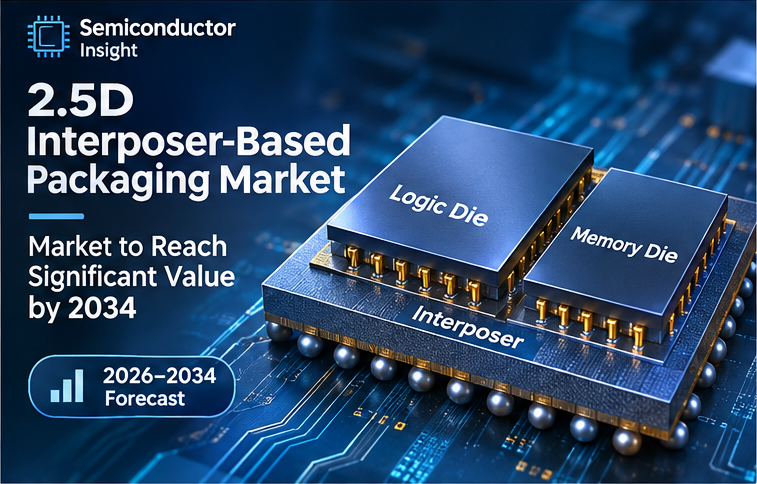
Interposer-based 2.5D assemblies typically place a large logic die beside high-bandwidth memory above an intermediate routing layer. Fine metal traces, microbumps, through-silicon vias and redistribution structures connect the dies to the underlying package substrate.
The interposer does not perform an independent computing workload, but it is a performance-critical part of the completed package. The market includes interposer fabrication, joining, assembly and associated package integration, rather than the full selling price of processors, memory chips or finished servers.
Silicon Interposers Continue to Lead the Technology Landscape
Silicon interposers account for an estimated 86% of type-related market value, reflecting established fine-line routing and through-silicon via manufacturing processes. Glass interposers represent approximately 14% and remain an emerging alternative for selected large-area and high-density designs.
Silicon offers established process control and manufacturing experience, while glass may provide dimensional stability and electrical advantages in selected applications. Glass adoption depends on reliable fine-hole formation, metallization adhesion, conductive vias and package-level mechanical qualification.
Data Centers Are the Largest End-User Segment
Data centers account for an estimated 67% of end-user market value, followed by consumer electronics at approximately 20% and telecommunications at around 13%. AI and high-performance computing systems require dense connections between compute dies and memory stacks.
Package architects must balance bandwidth, signal integrity, thermal performance, test access and assembly cost. Larger interposers can support more connections but may increase warpage, handling complexity and the financial impact of yield loss.
Assembly Yield and Substrate Availability Remain Key Challenges
Commercial capacity depends on coordinated availability of interposer wafers, microbump attachment, underfill, substrates, memory stacks and final testing. The effective output of the supply chain is constrained by the least available qualified input.
Package scaling introduces challenges involving substrate warpage, thermal management, alignment and reliability. Manufacturers are increasing early test insertion and design co-optimization to reduce the risk of discovering defects after several high-value dies have been assembled.
Receive your Free Sample Report today: https://semiconductorinsight.com/download-sample-report/
Where Are the Biggest Opportunities Emerging?
High-performance computing, AI accelerators and mobile processors represent key application areas. Heterogeneous integration allows different dies to be manufactured using suitable process technologies and combined in one package, supporting more flexible system design.
Asia-Pacific leads with an estimated 56% share, followed by North America at approximately 21%, Europe at 12%, the Middle East and Africa at 6%, and South and Central America at 5%. Taiwan and South Korea remain important production centers, while US customers influence high-value package design requirements.
Access the Full Report for In-Depth Insights: https://semiconductorinsight.com/report/2-5d-interposer-based-packaging-market/
2.5D Interposer-Based Packaging Market Market Segmentation
The report evaluates the market by product or technology type and application, providing a detailed view of where products and services are deployed.
By type, the market is divided into:
Silicon Interposer
Glass Interposer
By application, the market covers:
High-Performance Computing
AI Accelerators
Mobile Processors
Others
This segmentation helps industry participants compare technology configurations and end-use requirements while identifying the product categories that shape market demand.
View the complete market segmentation and forecast: https://semiconductorinsight.com/report/2-5d-interposer-based-packaging-market/
Regional Market Outlook
Asia-Pacific leads interposer-based packaging with an estimated 56% share of 2025 activity. North America represents approximately 21%, Europe 12%, the Middle East and Africa 6%, and South and Central America 5%. Taiwan and South Korea anchor established production, while US system designers influence bandwidth and thermal specifications for high-value packages.
Competitive Landscape and Key Companies
The market includes specialized technology providers, manufacturers and companies serving the relevant semiconductor and advanced manufacturing ecosystem.
Semiconductor Insight identifies TSMC, Samsung Electronics, Intel Foundry, ASE Technology Holding, Amkor Technology, JCET Group, NVIDIA, AMD, Broadcom and Qualcomm. The report distinguishes packaging providers from design customers and adjacent technology participants. among the companies and organizations covered in the competitive landscape.
Competition is influenced by product performance, manufacturing capability, process qualification, reliability, customer support and the ability to meet specialized application requirements. The report also examines manufacturer positioning, product portfolios, market performance and competitive developments.
What Does the Market Report Cover?
The Semiconductor Insight study evaluates market size, revenue, competitive positioning, industry dynamics, segmentation and regional performance. It examines packaging types, applications, end users, interposer materials, integration approaches and the supply chain for interposer fabrication, assembly, substrate handling and testing.
The study also evaluates market drivers, challenges, restraints, industry developments, new product developments, mergers and acquisitions, expansions and collaboration or supply arrangements where covered by the report.
Key Questions Answered by the Study
The report helps industry participants evaluate questions including:
How large is the 2.5D interposer-based packaging market?
Why are interposers used between logic and HBM?
Which interposer type currently leads?
Which end-user segment leads demand?
What factors constrain market expansion?
Explore the full market forecast and competitive analysis: https://semiconductorinsight.com/report/2-5d-interposer-based-packaging-market/
Get a Sample Report copy for free: https://semiconductorinsight.com/download-sample-report/
About Semiconductor Insight
Semiconductor Insight provides market intelligence and industry research covering semiconductor technologies, electronic components, advanced manufacturing systems and related technology markets. Its research focuses on market sizing, forecasting, competitive landscapes, technology trends, segmentation and regional analysis to support strategic decision-making across the semiconductor ecosystem.
Contact Semiconductor Insight
Website: www.semiconductorinsight.com


