

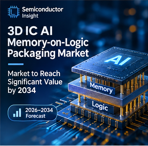
3D IC AI Memory-on-Logic Packaging Market to Reach USD 3,210.0 Million by 2034 as High-Density Vertical Integration Advances

The semiconductor industry is pursuing increasingly sophisticated packaging architectures as artificial intelligence workloads place greater pressure on memory bandwidth, interconnect density and energy efficiency. Against this backdrop, 3D IC AI memory-on-logic packaging is gaining attention because it vertically couples memory and compute functions through dense internal connections, potentially reducing the electrical distance between processing and data storage.
According to Semiconductor Insight, the 3D IC AI memory-on-logic packaging market generated USD 1,446.0 million in 2025 and is projected to reach USD 3,210.0 million by 2034, advancing at a CAGR of 9.3% over the 2026–2034 forecast period. Asia-Pacific accounts for an estimated 61% share, supported by the concentration of foundry, memory and heterogeneous assembly capabilities. The market covers qualifying vertical memory-on-logic packages and related integration services rather than all HBM components or complete AI servers.
Explore the complete market analysis: https://semiconductorinsight.com/report/3d-ic-ai-memory-on-logic-packaging-market/
Why Is This Market Becoming Important?
Memory bandwidth has become a critical consideration in AI accelerator design because processors must move large volumes of data between compute units and memory. Conventional board-level connections can create distance, power and bandwidth constraints, encouraging developers to evaluate denser package-level integration.
Memory-on-logic packaging places an active memory structure vertically with a compute die and connects the functions through high-density interfaces. Through-silicon vias, micro-bump joining and direct copper hybrid bonding can provide alternative or complementary routes for creating these connections.
The architecture can support wide parallel communication and shorter signal paths, but performance depends on thermal management, signal integrity, known-good die screening and final package yield. The value proposition therefore extends beyond stacking components; it requires coordinated design, bonding, inspection and testing.
Vertical Die Integration Is Expanding the Advanced Packaging Landscape
The report identifies micro-bump chiplet assemblies as the largest type segment, representing an estimated 43% of market value. TSV-based 3D ICs account for approximately 31%, while hybrid bonding solutions contribute around 26%. These categories distinguish the principal package configuration, even when individual products combine multiple interconnect techniques.
Micro-bump processes benefit from established assembly experience, while copper-to-copper hybrid bonding can support finer connection pitches. TSV structures provide vertical electrical paths through silicon and are used in several 3D architectures. Selection depends on interface density, manufacturing yield, thermal behavior and qualification requirements.
AI Accelerators Are Driving Memory-on-Logic Demand
Data-center AI accelerators represent the leading application, accounting for an estimated 58% of demand. High-performance computing contributes around 23%, edge inference approximately 12%, and autonomous vehicle computing about 7%. These applications require different balances of bandwidth, latency, power consumption and package cost.
Not every AI accelerator using high-bandwidth memory qualifies as memory-on-logic packaging. Many commercial systems place HBM beside logic on a 2.5D interposer. The report distinguishes these lateral arrangements from packages in which memory is vertically integrated with logic, making physical architecture an important factor in market measurement.
Thermal Design and Qualification Remain Critical
Dense vertical integration creates challenges involving heat removal, die alignment, bonding quality and package-level reliability. When active compute sits beneath memory, thermal design must account for power density and the impact of operating temperature on adjacent layers.
Known-good die testing is also important because defects discovered after expensive dies are bonded together can increase material losses. Manufacturers must monitor bonding voids, copper alignment, package warpage and electrical performance across wafer-level and final package tests.
Receive your Free Sample Report today: https://semiconductorinsight.com/download-sample-report/
Where Are the Biggest Opportunities Emerging?
Chiplet-based heterogeneous integration represents an estimated 63% of market value, compared with approximately 22% for monolithic 3D stacking and 15% for package-on-package hybridization. This reflects the growing use of modular dies and specialized assembly approaches in complex compute systems.
Asia-Pacific leads with an estimated 61% share, supported by Taiwan's advanced foundry ecosystem and South Korea's memory and packaging capabilities. North America contributes approximately 24%, Europe 10%, South and Central America 3%, and the Middle East and Africa 2%.
Access the Full Report for In-Depth Insights: https://semiconductorinsight.com/report/3d-ic-ai-memory-on-logic-packaging-market/
3D IC AI Memory-on-Logic Packaging Market Market Segmentation
The report evaluates the market by product or technology type and application, providing a detailed view of where products and services are deployed.
By type, the market is divided into:
TSV-Based 3D ICs
Micro-bump Chiplet Assemblies
Hybrid Bonding Solutions
By application, the market covers:
Data-Center AI Accelerators
Edge Inference Devices
Autonomous Vehicle Compute
High-Performance Computing (HPC)
This segmentation helps industry participants compare technology configurations and end-use requirements while identifying the product categories that shape market demand.
View the complete market segmentation and forecast: https://semiconductorinsight.com/report/3d-ic-ai-memory-on-logic-packaging-market/
Regional Market Outlook
Asia-Pacific leads the market with an estimated 61% share, supported by Taiwan and South Korea's advanced foundry, memory and assembly ecosystems. North America represents approximately 24%, reflecting accelerator design and cloud procurement activity. Europe accounts for around 10%, with specialist equipment, inspection and industrial applications contributing to the region. South and Central America and the Middle East and Africa represent smaller shares of approximately 3% and 2%, respectively.
Competitive Landscape and Key Companies
The market includes specialized technology providers, manufacturers and companies serving the relevant semiconductor and advanced manufacturing ecosystem.
Semiconductor Insight identifies TSMC, Samsung Electronics, ASE Technology Holding, Intel Foundry, Micron Technology, SK hynix, Cadence, Amkor Technology, GlobalFoundries and other advanced assembly partners. among the companies and organizations covered in the competitive landscape.
Competition is influenced by product performance, manufacturing capability, process qualification, reliability, customer support and the ability to meet specialized application requirements. The report also examines manufacturer positioning, product portfolios, market performance and competitive developments.
What Does the Market Report Cover?
The Semiconductor Insight study evaluates market size, revenue, competitive positioning, industry dynamics, technology segmentation and regional performance. It examines the value chain spanning foundry production, memory inputs, bonding, assembly, inspection and final package testing, while distinguishing qualifying memory-on-logic products from conventional side-by-side HBM packages.
The study also evaluates market drivers, challenges, restraints, industry developments, new product developments, mergers and acquisitions, expansions and collaboration or supply arrangements where covered by the report.
Key Questions Answered by the Study
The report helps industry participants evaluate questions including:
What is the size of the 3D IC AI memory-on-logic packaging market?
How does memory-on-logic differ from a standard HBM accelerator?
Which package type holds the largest share?
Which applications create the most demand?
Which region dominates the market?
Explore the full market forecast and competitive analysis: https://semiconductorinsight.com/report/3d-ic-ai-memory-on-logic-packaging-market/
Get a Sample Report copy for free: https://semiconductorinsight.com/download-sample-report/
About Semiconductor Insight
Semiconductor Insight provides market intelligence and industry research covering semiconductor technologies, electronic components, advanced manufacturing systems and related technology markets. Its research focuses on market sizing, forecasting, competitive landscapes, technology trends, segmentation and regional analysis to support strategic decision-making across the semiconductor ecosystem.
Contact Semiconductor Insight
Website: www.semiconductorinsight.com


